EN
EN



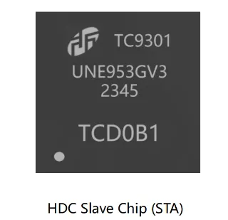
Digital chip design has become the foundation of modern high-volume integrated circuit development, enabling manufacturers to create millions of chips efficiently while maintaining quality and performance standards. The application of digital chip design methodologies across high-volume production environments represents a critical intersection of engineering precision and manufacturing scalability. As demand for semiconductors continues to rise across industries, understanding how digital chip design drives IC development at scale has become essential for engineers, product managers, and technology leaders.
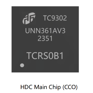
The path from conceptual design to mass production involves sophisticated tools, verified methodologies, and continuous optimization cycles. Digital chip design techniques ensure that each chip meets functional specifications, power requirements, and timing constraints before fabrication begins. This article explores how digital chip design principles translate into practical applications that support high-volume IC development and maintain competitive advantage in today's semiconductor landscape.
Design Methodology and Hardware Description Language Simulation
Foundation of Modern Chip Architecture
Hardware description language simulation forms the backbone of contemporary digital chip design practices. Engineers use HDL to describe chip behavior, logic structures, and functionality before physical implementation. This approach allows teams to verify digital chip design concepts through simulation, catching errors early and reducing costly iterations during fabrication.
Hardware description language simulation enables designers to model complex interactions between millions of transistors in a controlled virtual environment. By simulating chip behavior under various operating conditions, teams validate logic correctness, timing relationships, and power consumption predictions. For high-volume IC development, this stage determines whether designs are manufacturable at scale and meet performance targets.
Simulation-Driven Verification Processes
The verification phase relies heavily on hardware description language simulation to ensure integrated circuit verification across all functional modes and corner cases. Test benches created in HDL languages simulate real-world operating scenarios, stress conditions, and edge cases before chips enter production. This comprehensive testing approach significantly reduces defect rates in high-volume manufacturing environments.
Integrated circuit verification through simulation identifies potential design flaws that would otherwise appear only after fabrication. Engineers can validate timing compliance, signal integrity, and functional correctness within weeks rather than months. This efficiency gain becomes particularly valuable when scaling production to thousands or millions of units monthly.
VLSI Layout Optimization for Production Scalability
Physical Design and Layout Strategy
VLSI layout optimization transforms verified digital chip designs into physical layouts suitable for high-volume manufacturing. This process balances competing demands: minimizing chip area to reduce costs, optimizing power distribution for thermal management, and maintaining signal integrity across interconnects. Expert layout engineers use specialized tools to place and route millions of circuit elements efficiently.
The physical realization of digital chip design requires meticulous planning of metal layers, via connections, and signal paths. VLSI layout optimization techniques reduce parasitic capacitance and resistance that could degrade performance. For high-volume IC development, achieving optimal layouts across thousands of chip variants ensures consistent quality and manufacturing yield.
Manufacturing-Aware Design Implementation
Modern VLSI layout optimization incorporates design-for-manufacturability principles that anticipate fabrication process variations. Engineers design layout patterns that remain functional even when manufacturing tolerances shift slightly. This resilience proves critical when producing chips at high volumes, where process variations accumulate across millions of units.
Digital chip design teams collaborate closely with foundry partners to understand process capabilities and constraints. VLSI layout optimization leverages this knowledge to maximize yield, minimize defects, and ensure consistent performance across production batches. This collaboration transforms theoretical designs into reliable products that function reliably in customer applications.
Integrated Circuit Verification and Quality Assurance
Comprehensive Testing Frameworks
Integrated circuit verification encompasses far more than simulation alone. Physical testing of fabricated chips validates that theoretical designs translate accurately into silicon. Test engineers develop comprehensive test suites that exercise every functional path and validate performance specifications before chips ship to customers.
For high-volume IC development, integrated circuit verification must be fast, thorough, and economically efficient. Automated test equipment rapidly screens chips for defects, timing violations, and functional errors. This automated approach enables manufacturers to maintain quality standards while processing millions of chips through production facilities monthly.
Yield Optimization and Continuous Improvement
Integrated circuit verification data feeds directly into yield optimization programs that improve production processes continuously. By analyzing defect patterns and performance variations, engineers identify root causes and implement corrective measures. This closed-loop approach ensures that digital chip design refinements result in measurable improvements in yield and reliability.
High-volume IC development succeeds when manufacturers treat verification not as a final checkpoint but as an ongoing learning process. Each production batch provides insights that inform next-generation digital chip design improvements. Teams analyze yield data, investigate anomalies, and implement process enhancements that compound into significant reliability and cost advantages over time.
FAQ
How does hardware description language simulation improve digital chip design quality?
Hardware description language simulation allows engineers to verify digital chip design functionality before fabrication, catching logic errors and timing violations early. By simulating millions of operating conditions virtually, teams identify and fix problems that would otherwise appear as expensive defects in manufactured chips. This simulation-based approach reduces development time and improves final product reliability significantly.
Why is VLSI layout optimization critical for high-volume IC development?
VLSI layout optimization ensures that digital chip design concepts translate into manufacturable physical layouts that maintain performance across process variations and high-volume production. Optimized layouts reduce area, improve power efficiency, and enhance yield rates. For manufacturers producing millions of chips, small optimization improvements compound into substantial cost savings and competitive advantages.
What role does integrated circuit verification play in ensuring production quality?
Integrated circuit verification validates that fabricated chips meet functional and performance specifications through comprehensive testing. This verification stage catches defects early, prevents customer failures, and provides feedback for continuous process improvement. In high-volume manufacturing, robust integrated circuit verification protects reputation and maintains customer satisfaction across millions of units produced.